These are notes I’ve collected while designing Agatha and a few other PCIe board. I’ve included sources where possible, but a lot of the other stuff summaries from Stack Overflow and forum posts.
Even if anything below actually works, don’t take any of it as gospel unless it cites an authoritative source. That’s my disclaimer.
---
Resources
Cadence - PCIe Design Guide – Q&A (Gen 4, 5, 6) - Part 1
Sierra Circuits - 10 Best High-Speed PCB Routing: PDF Version / mhtml version
Stackups
See PCIe Stackups.
PCIe Power Pins
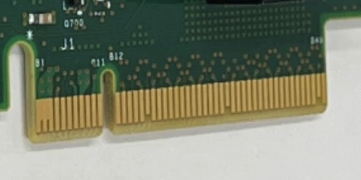
It’s acceptable to bridge the power pins within the edge connector itself! The ORACLE 7096186/NVMSW8 card does it (but don’t get that card itself, it only works on certain machines).
Current Requirements
All cards, regardless of slot width, can consume 3v3 at 3A. 12V depends on card width.
| Width | 3v3 Amps | 12v Amps | Combined Max Watts |
|---|---|---|---|
| x1 | 3 | 0.5 | 10 |
| x4 | 3 | 2.1 | 25 |
| x8 | 3 | 2.1[1] | 25 |
| x16 | 3 | 5.5 | 75 |
| 1: I couldn’t find any specific info on x8, so I’m assuming it’s the same as x4. |
Traces
hMeasurementHere,
his the dielectric thickness between the trace and its reference plane. For OSHPark, the 4-layer dielectric thickness between layers is 0.2mm. Therefore, the minimum spacing between pairs of the same net is 0.8mm (4h).
Avoid traces running parallel with PCB grain
Avoid running long traces in parallel with grain of the fiber. (emphasis mine) — Slide 5
Differential Skew
Trace mis-match compensation should be done at the point of mis-match. — Slide 8
Serpentines
Multiple small sections instead of one farm (better for Gen3) - Differential Pair Length Matching: Best Practices for Signal Integrity | Blog | Altium
+ trace:  ---/\/\-----------/\/\-----------/\/\---
- trace:  ----------------------------------------
PCIe Versions and Serpentines
- 🟢 Gen3
- Multiple small sections are recommended because they reduce discontinuities and keep coupling more uniform.
- 🟡 Gen4
- Multiple small sections are strongly recommended because the eye margin is tighter and long meanders start to behave like a filter.
- 🔴 Gen5
- Multiple small sections are effectively required. A single large serpentine is almost always a layout violation in real Gen5 designs.
- This is because serpentines behave like filters at high frequency. At Gen5, this can create resonant notches in the insertion loss.
- Most Gen5 layout guides explicitly say:
- Keep tuning sections short and sparse
- Avoid dense meanders
- Maintain tight coupling through tuning
- Distribute tuning near each mismatch, not in one big block
🎯 The rule of thumb I give layout engineers
If you can see the serpentine from across the room, it’s too big for Gen4/Gen5.
Short, sparse, distributed tuning is the only safe pattern.
(Source: Copilot)
Inter-Pair Spacing
Between Pairs for different lanes
Inter-pair spacing (between TX and RX pairs of different lanes):
- Minimum spacing:
- Keep ≥3h (stripline) or ≥4h (microstrip) between differential pairs of
different lanes.
- For Gen3, use ≥4h where feasible to avoid near-end crosstalk (NEXT) due to PAM4’s tighter eye margins.
- This is the same rule of thumb as for TX vs RX of the same lane, but applied across lanes.
- Keep ≥3h (stripline) or ≥4h (microstrip) between differential pairs of
different lanes.
- Preferred spacing:
- If PCB real estate allows, increase spacing to 5h-6h between lanes. This provides extra margin for high-speed signaling and reduces lane-to-lane interference.
- Routing considerations:
- Avoid running long parallel segments of different lanes close together. If unavoidable, introduce staggering or ground shielding traces.
- Maintain consistent spacing across the entire channel (don’t bunch lanes together near connectors or vias).
- Keep lane groups aligned and length-matched, but still respect isolation spacing.
Between Pairs for the same lane
Inter-pair spacing (between TX and RX pairs of the same lane):
To reduce crosstalk between the transmit and receive pairs, guidelines recommend:
- Microstrip (outer layer traces): ≥4h spacing
- Stripline (inner layer traces): ≥3h spacing
Spacing from non-Differential signals
Keep at least 4h away from unrelated signals.
If those signals have higher slew rates or voltage swings, increase spacing to 6h.
Critical Signals (e.g., REFCLK, PERST#, SMBus): Maintain ≥5x trace width separation from high-speed aggressors. Sensitive control signals can pick up noise that triggers false resets, clock modulation, or margin loss.
For “clean” (well-decoupled) power traces, 3h might be sufficient but 4h is preferred.
Via Fences
For a PCIe 3.0 pcb, a good rule of thumb for via fence spacing is to use a spacing of 1/10th of the wavelength of the highest frequency of interest to create a continuous ground shield. For PCIe 3.0, which operates at 8 GT/s (gigatransfers per second), this often translates to a via-to-via spacing of approximately 3 to 5 mm to prevent EMI and maintain signal integrity, though specific designs may vary. — Gemini
For PCIe 4.0, which operates at high frequencies (up to ~8 GHz), via fence spacing should be very tight, often around 3.75 mm or less (1/20th of the ~7.5 cm wavelength for 4 GHz) for stitching vias to act as a ground plane, ensuring effective shielding, with minimum via-to-via spacing typically 0.2-0.3 mm edge-to-edge, always respecting your PCB manufacturer’s capabilities for signal integrity.
Minimum Edge Clearance (DFM)
To prevent damage during the profiling (cutting) process, use these minimum distances from the via hole edge to the PCB board edge:
- Standard Routed Edge: 0.5 mm is the industry recommended minimum to prevent “broken holes” during board profiling.
- V-Scored Edge: 1.0 mm is required if the board is separated via V-scoring, as the scoring blade can easily damage or cut through vias placed too close to the edge.
- Copper-to-Edge Rule: Most manufacturers require a general copper-to-edge clearance of at least 0.25 mm to 0.5 mm to avoid exposing copper during the milling process.
— Gemini
Edge Connector
Inner Ground Plane Keepout
For PCIe 3.0 cards, the recommended gap between the ground plane and the edge connector fingers-often referred to as the “keep-out” region-is typically 1.0 mm to 1.5 mm.
Card Slot
For PTH connectors, inner ground plane layers should extend underneath the connector.
There appears to be no prohibition on extending the ground fill on the bottom copper to the be underneath the PCIe connector as well. I am not sure about fill on the top layer.
AC Coupling Capacitors
I’m not using them now, because they should be on the PCIe device, but here’s a discussion about them for the future: high frequency - Backwards compatibility of PCIe AC coupling capacitors - Electrical Engineering Stack Exchange